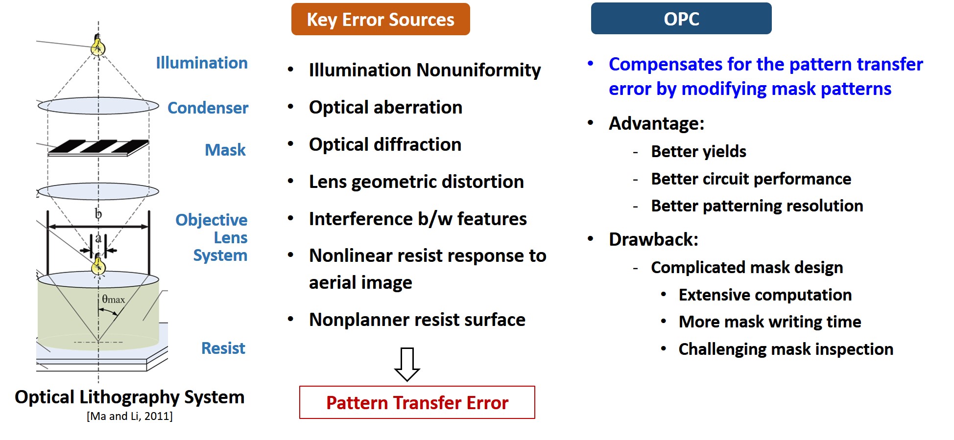
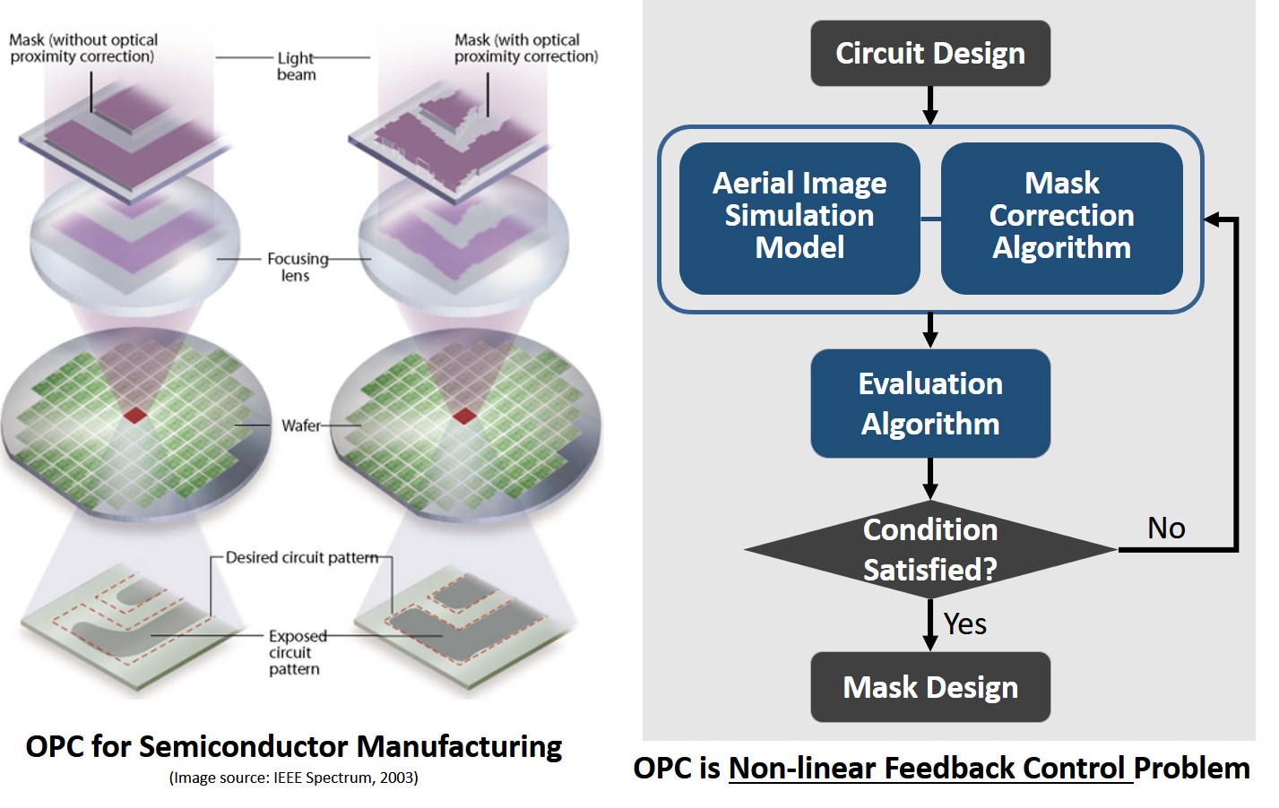
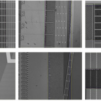
In order to transfer desired circuit patterns onto wafer accurately using optical lithography, we need to consider various factors such as illumination, optics, mask, resist, etch, and positioning system. Instead of making them perfect, optical proximity correction (OPC) can be used to modify mask geometries to compensate for pattern transfer non-idealities. It is used to obtain better edge placement and more accurate CD to achieve higher yield, better circuit performance, and adoption of smaller design rules. Because of this reasons, OPC is considered as one of the resolution enhancement techniqies (RET) for optical lithographic processes. It simulates imaging system model described by Hopkins equation and improves the mask image and reduces pattern transfer error at the resist surface by optimiing the mask shape. When Dr. Kang worked for Intel as a RET design engineer, he developed various OPC techniques for Intel's current and next generation process technologies.
