Plastic ball grid array (PBGA) is one of the most widely used types of chip packages in various electronic devices such as network servers, microcontrollers, and memory devices. As the demand for higher performance electronic devices grows, the I/O densities of PBGA packages are increasing while requiring superior reliability. Warpage induced during the reflow assembly process is one of the crucial factors affecting the thermo-mechanical reliability of PBGA packages; therefore, accurate warpage prediction is an important task for package design processes. In this study, the effects of four geometric factors (the solder bump pitch,package size, and molding compound and substrate thicknesses) of the PBGA package on its warpage are assessed by using parametric finite element analysis. The study employed the Taguchi method to design simulations and ANOVA to identify the effects of each factor on the PBGA warpage. For the particular PWBA model used in this study, it is found that the solder bump pitch, package size, and molding compound thickness affect the maximum PBGA warpage significantly but the substrate thickness does not. Numerical models to estimate the warpage affected by the four factors are developed using the regression method. The adjusted R2 values of the models were higher than 92%. The results of this study are expected to provide guidelines that in-house PBGA designers can use to meet the warpage requirements of PBGA packages.
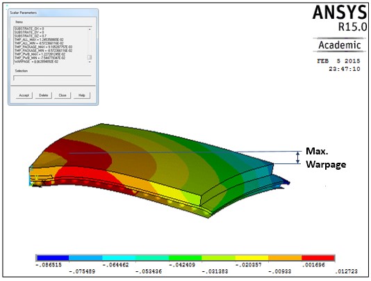
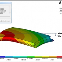
A warpage contour plot generated by ANSYS

