Skip to menu

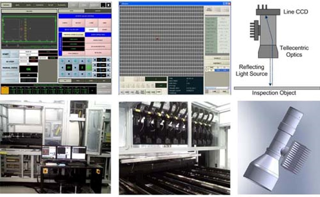
Low defect detectability and complex calibration hampered Samsung’s existing optical inspection and repair systems used for the automation and quality control of their LCD manufacturing process. To solve this problem, Dr. Kang developed an automatic optical inspection (AOI), including its core techniques and software, which inspects for defects on 2500 mm by 2200 mm LCD panel with 15 µm resolution and 99% detectability and within 60 seconds, and automatically repair disconnected or narrow sealants dispensed on the panel. Because of the high accuracy, speed, and robustness of my AOI system, Samsung bought it at a cost of approximately $1 million per system over several competitors. As the project manager for three years, his leadership allowed his team of three graduate students and three engineers to develop this innovative and high performance AOI system.


Completed Research Topics:

  • Robust and fast image processing algorithm for LCD defect detection
  • In-process coordinate calibration method between the moving stage, twelve line-scan cameras, and LCD panel.
  • Telecentric objective lens and LED light source for line-scan cameras to obtain high-qulity LCD panel image
  • Communication method between the twelve line-scan cameras
  • Image buffering method for very fast real-time image processing
  • Transmitter to produce high-frequency signal to synchronize high-speed motion and camera scanning.  
  • Control and image processing programs using C++
 aoi01.jpg

The Automatic Optical Inspection System


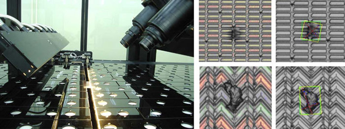
Before developing the AOI system sold to Samsung, Dr. Kang performed several research topics for LCD defect inspection. For example, he intially devloped a desktop type machine vision system with area camera to capture and detect LCD defects. Then, he devloped another AOI system that consists of air floating bed, inclined line scan cameras, and hallogen and metal-halide light source.


Completed Research Topics:

  • Reflected and tranmitted halogen lighting for scanning LCD panels
  • Air floating bed for transffering large LCD panels
  • Pattern elimination algorithm using 1D FFT
  • Fast geometric analysis algorithm to identify detected defects
 aoi02.jpg 

The Automatic Optical Inspection System with Air Floating Bed and Inclined Cameras


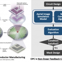
  1. Optical proximity correction technique for enhancing the resolution of Intel's optical lithographic process

    In order to transfer desired circuit patterns onto wafer accurately using optical lithography, we need to consider various factors such as illumination, optics, mask, resist, etch, and positioning system. Instead of making them perfect, optical proximity correction (OPC) can be used to modify mask geometries to compensate for pattern transfer non-idealities. It is used to obtain better edge placement and more accurate CD to achieve higher yield, better circuit performance, and adoption of smaller design rules. Because of this reasons, OPC is considered as one of the resolution enhancement techniqies (RET) for optical lithographic processes. It simulates imaging system model described by Hopkins equation and improves the mask image and reduce...
    Read More
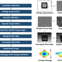
  2. In-process 3D measurement for semiconductor assembly using fringe projection technique

    Warpage is the microscale 3D deformation of the surface of semiconductor packages generated during the thermal reflow process for assembling the packages on a printed circuit board (PCB). Because warpage affects the reliability of the packages, its accurate measurement and control are important tasks during the reflow process. Shadow moiré and laser moiré techniques are commonly used for measuring warpage. However, the shadow moiré technique cannot be used for simultaneously measuring the warpage of the assembled package and the PCB because it requires a glass grating located very close to the sample, and the laser moiré technique has a critical error source of laser speckle. These techniques also require spraying...
    Read More
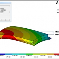
  3. Parametric studies of effects of geometric factors on warpage of PBGA packages

    Plastic ball grid array (PBGA) is one of the most widely used types of chip packages in various electronic devices such as network servers, microcontrollers, and memory devices. As the demand for higher performance electronic devices grows, the I/O densities of PBGA packages are increasing while requiring superior reliability. Warpage induced during the reflow assembly process is one of the crucial factors affecting the thermo-mechanical reliability of PBGA packages; therefore, accurate warpage prediction is an important task for package design processes. In this study, the effects of four geometric factors (the solder bump pitch,package size, and molding compound and substrate thicknesses) of the PBGA package on its warpage are assessed by ...
    Read More
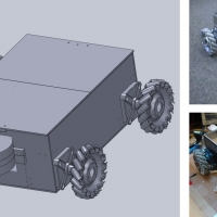
  4. Smart Omnigro: Omni-directional intelligent ground robot

    In this project, Smart Omnigro, an unmanned ground vehicle to act as a tool for intelligence, surveillance and reconnaissance which has obstacle avoidance and smartphone control functions is developed. Omni-directional wheels are used for steering and motion strategy. Software algorithm using potential field utilizing GPS and untrasonic sensor signals, which give the information of the robot coordinate and obstacle positions around the robot respectively, is developed for path planning avoiding obstacles. A noble control interface is developed to monitor and control the robot using smartphones through the internet. As a result of the successful development in this project, the robot incorporating with an unmmend aerial vehicle won the first ...
    Read More
  5. In-process defect inspection for LCD manufacturing using optical and machine vision techniques

    Low defect detectability and complex calibration hampered Samsung’s existing optical inspection and repair systems used for the automation and quality control of their LCD manufacturing process. To solve this problem, Dr. Kang developed an automatic optical inspection (AOI), including its core techniques and software, which inspects for defects on 2500 mm by 2200 mm LCD panel with 15 µm resolution and 99% detectability and within 60 seconds, and automatically repair disconnected or narrow sealants dispensed on the panel. Because of the high accuracy, speed, and robustness of my AOI system, Samsung bought it at a cost of approximately $1 million per system over several competitors. As the project manager for three years, his leade...
    Read More
  6. Automatic classification of LCD defects using machine learning techniques

    Defect control is one of the critical parts for quality control in LCD manufacturing process and there are three main steps for the defect control, which are defect detection, defect classification, and removal of defect sources. Defect classification is a necessary step to identify the sources of detected defects, and it typically relies on human visual judgement, whicih iincreses the overall manufacturing time. To solve this problem, Dr. Kang developed an automatic defect classification method using support vector machine and neural network machine learning algorithms. The experimental results showed 86.409% classification accuracy to classify four main yield-producing particle defects. Completed Research Topics: Defining 24 features to cl...
    Read More
  7. In-Process measurement and repair of sealant on LCD glasses

    During the LCD manufacturing, sealant is printed on a color filter glass and is then adhered to a thin film transistor glass. Liquid crystal is then filled into the space between the two glasses, which is sealed by the sealant. Because missing or narrow sealant causes leakage of the liquid crystal, its detection and repair are important tasks during the LCD manufacturing. In this project, Dr. Kang developed a processing algorithm to segment sealant regions over complex LCD patterns using frequency domain analysis. Also, he developed a sealant repair system to repair missing or narrow sealant with 40um resolution. Examples of Result Images of Sealant Segmentation (green lines shown on the images are the segmentation result) The Sealant Repair...
    Read More
Board Pagination Prev 1 Next
/ 1